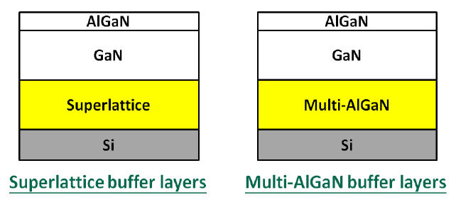
Gallium Nitride on Silicon wafer we can provide the wafer material for both 5F/RF and Power application, D-mode GaN-on-Si HEMT & E-mode GaN-on-Si HEMT with our Superlattice buffer and Multi-AlGaN buffer layers.
*Very low particle count
*Crack-free EPI wafer
*High lateral breakdown voltage
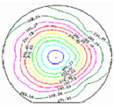
*Excellent thickness and composition uniformity
*High breakdown voltage and low leakage current characteristics
|
Wafer Size |
4~6" GaN on Si wafer |
|
|
Silicon thickness |
675/1000 |
um |
|
GaN cap thickness |
2 |
nm |
|
AlGaN barrier thickness |
20~25 |
nm |
|
Al content of AlGaN barrier |
20~30 |
% |
|
AlN spacer thickness |
1 |
nm |
|
Epi total thickness |
<4000 |
nm |
|
Wafer bow |
±50 |
μm |
|
FWHM of GaN(002) |
<700 |
arcsec |
|
FWHM of GaN(102) |
<700 |
arcsec |
|
*all can be customizable |
||