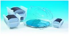
Silicon wafer is the most common material and widely used for a variety of high-tech industries, including integrated circuits , detector or sensor device , MEMS fabrication, opto-electronic components, and solar cells .
|
Silicon Wafer Specification |
||
|
Diameter |
100- 300mm |
|
|
Growth |
P-Type |
Boron |
|
Dopant |
N-Type |
Arsenic / Antimony / (Red) Phosphorus |
|
Thickness |
150 ~ 1500um, Customizable |
|
|
Surface |
Ingot / As Cut / Lapped / Etched / Polished |
|
|
Float Zone FZ-Silicon Specification |
||||
|
Parameter |
Conduction Type |
Orientation |
Diameter(mm) |
Resistivity(Ω.cm) |
|
High Resistivity |
P-Type |
<100>&<111> |
125-200 |
>1000 |
|
Neutron Radiation |
30-800 |
|||
|
CFZ |
N-Type |
1-50 |
||
|
Meteorological Adulteration |
0.01-300 |
|||
|
(Magnet) Czochralski MCZ/CZ-Silicon Specification |
||||
|
Parameter |
Conduction Type |
Orientation |
Diameter(mm) |
Resistivity(Ω.cm) |
|
Light Dopant |
P-Type |
<100><111> |
76.2-300 |
1-100 |
|
Heavy Dopant |
N-Type |
0.0005-1 |
||